
Introduction
Semiconductor wafers are the foundation of every modern electronic system—from smartphones and data centers to electric vehicles and aerospace systems. Behind every chip lies a highly sophisticated manufacturing process that transforms ordinary sand into billions of nanoscale transistors. This article provides a step-by-step overview of the semiconductor wafer manufacturing process, typical complexity involved, major industry challenges, and a concluding perspective on why this domain is strategically critical.
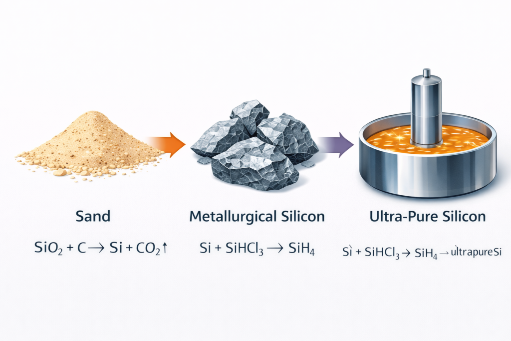
1. Silicon Extraction: From Sand to Ultra-Pure Material
The journey begins with silicon dioxide (SiO₂), commonly found in sand and quartz. Through a high-temperature carbothermic reduction process, silicon dioxide is converted into metallurgical-grade silicon with approximately 98–99% purity.
To reach semiconductor-grade purity, silicon undergoes chemical purification using processes such as the Siemens method. Silicon is converted into volatile compounds like trichlorosilane, distilled, and re-deposited as ultra-pure polysilicon. The final purity can reach 9N to 12N (99.999999999% or higher), which is essential for reliable semiconductor devices.
2. Single Crystal Growth: Polysilicon to Silicon Ingot
Integrated circuits require single-crystal silicon to ensure predictable electrical properties. Two primary crystal growth methods are used:
- Czochralski (CZ) Method: The most widely used method, where a seed crystal is dipped into molten silicon and slowly pulled to form a cylindrical single-crystal ingot.
- Float Zone (FZ) Method: Used mainly for power electronics and RF devices, offering higher purity due to the absence of crucible contamination.
3. Wafer Slicing: Ingot to Thin Silicon Disks
The cylindrical silicon ingot is shaped and sliced into thin wafers using diamond wire saws. Typical wafer diameters are 200 mm and 300 mm. After slicing, wafers undergo edge rounding to improve mechanical strength and reduce cracking risks.
4. Wafer Polishing and Cleaning
Sliced wafers must have an atomically flat surface. This is achieved through:
- Lapping: Removes saw marks and thickness variations.
- Chemical Mechanical Polishing (CMP): Produces a mirror-like surface with nanometer-level flatness.
- RCA Cleaning: Removes organic contaminants, metals, and particles.
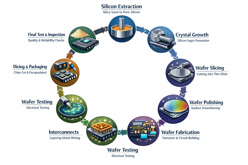
5. Wafer Fabrication: Building Transistors and Circuits
This is the core of semiconductor manufacturing, where transistors and interconnects are formed through hundreds to thousands of repeated process steps.
Key Process Cycles
Oxidation: High-temperature growth of silicon dioxide layers for insulation and gate dielectrics.
Photolithography: Photoresist is applied, exposed using DUV or EUV lithography masks, and developed to transfer circuit patterns onto the wafer.
Etching: Removes unwanted material using plasma-based dry etching or wet chemical etching.
Ion Implantation: Introduces dopants such as boron, phosphorus, or arsenic to create p-type and n-type regions.
Deposition: Adds material layers using techniques like CVD, PVD, and ALD for oxides, nitrides, polysilicon, and metals.
6. Transistor Formation (FEOL)
Modern transistor structures have evolved significantly:
- Planar MOSFET
- FinFET
- Gate-All-Around (GAA) / Nanosheet transistors
Key steps include gate stack formation, source/drain engineering, spacers, and strain engineering to enhance performance.
7. Interconnect Formation (BEOL)
Once transistors are formed, multiple metal layers are added to connect billions of devices. Low-k dielectrics, copper or cobalt interconnects, and CMP planarization are repeated across 10–15 or more metal layers in advanced nodes.
8. Wafer Testing (Electrical Wafer Sort)
Each die on the wafer is tested using probe cards to identify functional and defective chips. Results are stored in wafer maps for downstream processing.
9. Dicing: Wafer to Individual Chips
Diamond saws or laser dicing tools separate the wafer into individual dies.
10. Packaging and Final Test
Individual dies are packaged to provide protection and electrical connections. Packaging technologies include wire bonding, flip-chip, fan-out wafer-level packaging, and advanced 2.5D/3D integration. Final electrical and reliability tests ensure product quality before shipment.
Typical Manufacturing Complexity
| Parameter | Typical Value |
|---|---|
| Total process steps | 1,000–3,000+ |
| Manufacturing cycle time | 12–20 weeks |
| Tool cost per equipment | $1M–$20M+ |
| Fab construction cost | $10B–$30B+ |
| Cleanroom class | Class 1 or better |
| Layers in advanced chips | 50–100+ lithography layers |
Major Challenges in Wafer Manufacturing
1. Extreme Capital Intensity
Building and operating a semiconductor fab requires tens of billions of dollars and continuous technology upgrades.
2. Process Complexity and Yield
Thousands of steps with atomic-scale precision make defect control and yield optimization a constant challenge.
3. Lithography Scaling Limits
EUV lithography, multi-patterning, and stochastic defects create new challenges as feature sizes approach atomic limits.
4. Materials and Physics Limits
Leakage, variability, and quantum effects increasingly impact device reliability and performance at advanced nodes.
5. Supply Chain and Geopolitics
Semiconductor manufacturing depends on a globally distributed supply chain, making it vulnerable to geopolitical and logistical disruptions.
Conclusion
Semiconductor wafer manufacturing is one of the most complex and capital-intensive engineering achievements in modern industry. From sand purification to nanoscale transistor fabrication, every step requires precision, innovation, and massive infrastructure. As AI, EVs, and connected systems continue to grow, wafer manufacturing will remain a strategic backbone of global technology leadership. Understanding this process provides critical insight into the silicon-to-system value chain and the future of electronics innovation.


Leave a Reply